UV-LED exposure systems

UV-LED exposure systems for photolithography (UV-EXP series)

With the UV-EXP series, idonus offers an innovative UV illumination system based on the use of high-power LEDs and high-grade homogenization optics. This product line finds application in photoresist exposure (UV-LED photolithogaphy and curing) and is suitable for a wide variety of substrates and photoresists used in MEMS, microfluidics, photonics, semiconductors and photovoltaic applications. Our standard line of UV illumination products addresses photolithography needs for masks and wafers up to 300 mm wide (11.8 inches).

Customized solutions can be designed to suit your specific requirements (e.g., retrofitting of mask aligners, OEM for your future products). For further details on UV-LED retrofittings and custom exposure systems, see also our solutions > technologies page.


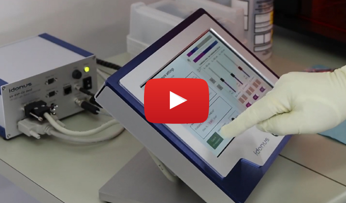
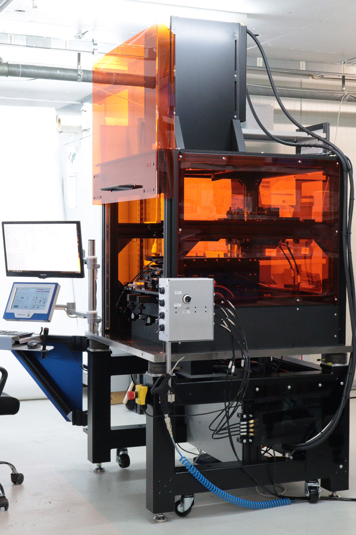
Watch this video to discover the features of the idonus UV-EXP Gen. 2 exposure systems.


Why LED technology?

Until recently, mercury arc lamps were the only sources capable of providing high intensity light suitable for UV photolithography exposure. Thanks to the advances in LED technology, UV-LEDs have become a very attractive alternative to the hazardous and energy-consuming mercury lamps.

Along with the ecological and security aspects, the technical advantages of UV-LEDs as compared with traditional mercury lamps are numerous and significant for photolithography. A foremost advantage of UV-LEDs is that they operate with consistent emission for very long lifetimes. As a result, daily calibration and maintenance are not required. Furthermore, by being more energy efficient, LEDs have reduced heating, which greatly simplifies system cooling.

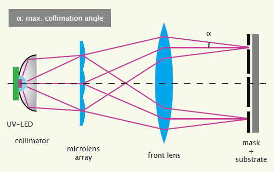
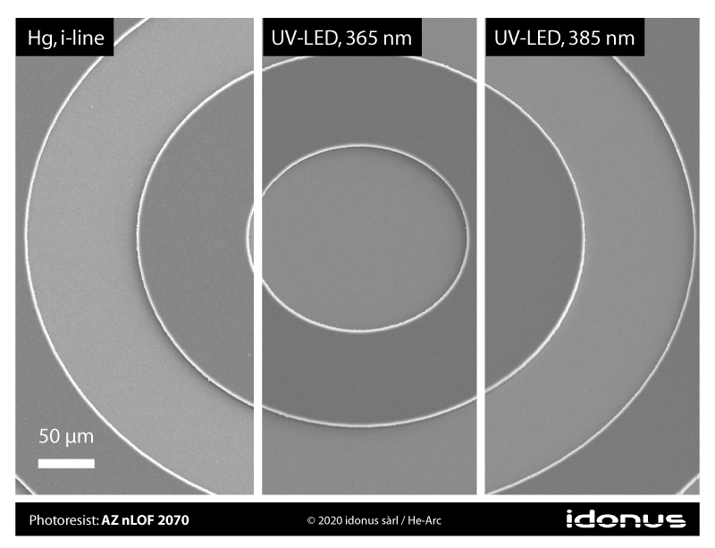
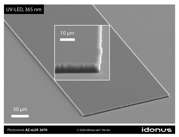
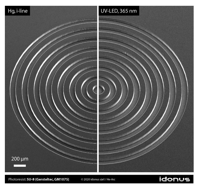
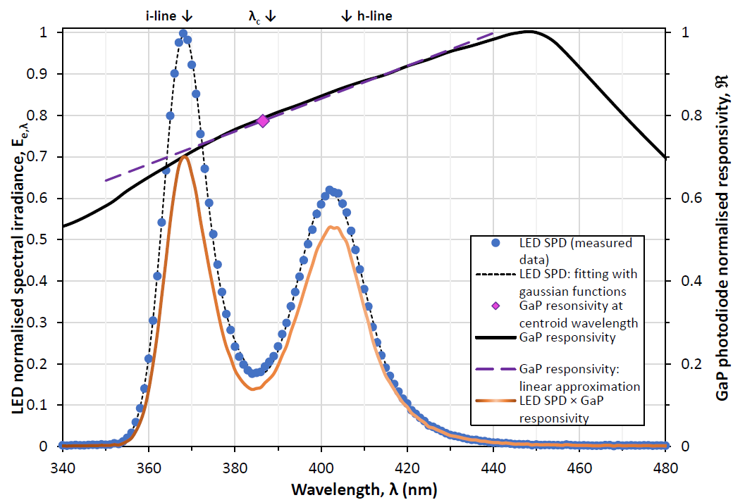
It is noteworthly that LEDs emitting at 365 nm, 405 nm and 435 nm (peak wavelengths) can be combined to mimic the UV-A spectrum of mercury-arc lamps (i-line, h-line and g-line characteristic peaks of Hg element), as can be seen in this graph.

Downloads


UV-EXP series product datasheet (PDF).

UV-EXP product flyer (PDF).

Technical note: UV-LED for photolithography exposure / Hg lamp retrofitting (PDF).

DOI: 10.13140/RG.2.2.31287.65446


Technical note: 
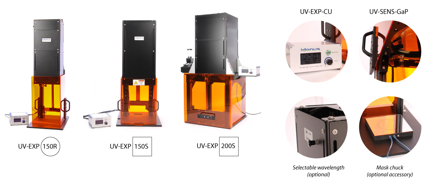
Photoresist exposure with the idonus UV-EXP equipment (PDF, preview).

Please, contact our sales team to receive the full version of our technical note on photoresist exposure.

Technical guide: LED technology for nonimaging optics (PDF).

DOI: 10.13140/RG.2.2.29958.32323

White Paper: Broadband radiometric measurement of LEDs (PDF, preview paper).

DOI: 10.13140/RG.2.2.34765.05600/2

Please, contact our sales team to receive the full version of this White Paper.

White Paper: Human vision and the CIE chromaticity diagram (PDF, preview paper).

Please, contact our sales team to receive the full version of this White Paper.


Useful references

"Investigating the pattern transfer fidelity of Norland Optical Adhesive 81 for nanogrooves by microtransfer molding," R. Sabahi-Kaviani and R. Luttge, J. Vac. Sci. Technol. B 39, 062810 (2021).
DOI: 10.1116/6.0001333

"Gaining Micropattern Fidelity in an NOA81 Microsieve Laser Ablation Process," R. Sabahi-Kaviani and R. Luttge, Micromachines, 2021, 12(1), 21.
DOI: 10.3390/mi12010021


Benefits of UV-LED exposure

  • Stable illumination, no daily calibration required
  • Instant-on, light is ON only during exposure, no mechanical shutter needed
  • Long lifespan, meaning no more consumable required
  • Narrow spectrum: no unwanted heating of the substrate and more repeatable process
  • low power consumption
  • no maintenance costs

idonus UV-LED exposure systems

idonus has introduced a complete line of UV-LED exposure products. Our systems integrate the most effective UV-LEDs available on the market together with high-grade microlens arrays. They are fully assembled and controlled in-house. Our design features a fully telecentric optics that provides reproducible and uniform illumination conditions over the whole exposure area – i.e., highly uniform and stable intensity with very small divergence angles. This cutting edge optics ensures perfectly uniform exposure of the entire substrate, producing cured photoresists with straight sidewalls and enabling precise microstructuring of patterns with micrometer critical dimensions.

Fig. A: Optical system (simplified) ● High uniformity of the illumination is achieved thanks to the use of a microlens array homogenizer.

Performance of the idonus UV-EXP

Our UV-LED exposure system is available in several standard configurations that can be customized with a multitude of variants and options (e.g., single or mixed wavelengths). As a manufacturer of special machines, idonus can also develop fully customized equipments according to client's specifications (e.g., different exposure area, adapted equipment housing). The main characteristics of our products are given in the Table "Standard UV-LED exposure systems".

A typical measurement performed during the calibration process is shown in Figure B . In the usable exposure area, irradiance non-uniformity, (max-min)/(max+min), is lower than 3%. The maximum collimation angle α which is illustrated in Figure A is another important parameter that we systematically characterize. Data shown in Figure C are typical results extracted from measurements performed on one of our models. To evaluate α, irradiance is measured as a function of the collimation angle: α corresponds to the FWHM (full width at half maximum). This threshold is commonly used to consider light energy effectively contributing to photoresist irradiation. Given the performance of our exposure system, about 95% of the energy is enclosed within the collimation angle α.


Fig. B1: Irradiance uniformity ● Exposure output from model UV-EXP100S (square illumination area of 100×100 mm²).


Fig. B2: Irradiance uniformity ● Measurements show non-uniformity lower than 3%. Typical values extracted from one of our models (UV-EXP100S, square illumination area of 100×100 mm²).


Fig. C: Collimation angle ● UV light is enclosed within the max. collimation angle α (intensity threshold at FWHM, corresponding to 95% of light energy). Typical values extracted from our UV-EXP150S (max. collimation angle α of ±1.8°, or 2α = 3.6°).


idonus standard UV-LED exposure systems
Model Wavelength Useful exposure area Irradiance, Ee Non-uniformity, C * αFWHM WD ** External dimensions, mm³
@385/395/405 nm @365 nm (lamphouse only) (complete system)
UV-LAB100R 365 nm Ø 100 mm 12 mW/cm² 5% ±2° 250 mm 200×250×400 250×300×670
UV-EXP150R 365 and/or 385 / 395 / 405 / 435 nm Ø 150 mm 50 mW/cm² 40 mW/cm² 3% ±1.8° 350 mm 610×305×250 1000×480×330
UV-EXP150S 365 and/or 385 / 395 / 405 / 435 nm 150×150 mm² 50 mW/cm² 40 mW/cm² 3% ±1.8° 300 mm 600×360×300 960×500×420
UV-EXP200R 365 and/or 385 / 395 / 405 / 435 nm Ø 200 mm 30 mW/cm² 25 mW/cm² 3% ±1.4° 400 mm 730×415×360 1170×570×530
UV-EXP200S 365 and/or 385 / 395 / 405 / 435 nm 200×200 mm² 30 mW/cm² 25 mW/cm² 3% ±1.4° 400 mm 730×415×360 1170×570×530
UV-EXP300S-1LE 365 and/or 385 / 395 / 405 / 435 nm 300×300 mm² 17 mW/cm² 13 mW/cm² 3% ±1.0° 300 mm 920×560×510 1270×715×700
UV-EXP300S-3LE 365 and/or 385 / 395 / 405 / 435 nm 300×300 mm² 50 mW/cm²
(3 LEDs)
40 mW/cm²
(3 LEDs)
3% ±2.5° 300 mm 920×560×510 1270×715×700
UV-EXP600S 365 and/or 385 / 395 / 405 / 435 nm 600×600 mm² 30 mW/cm²
(multiple LEDs)
20 mW/cm²
(multiple LEDs)
3% ±2.0° 300 mm 1500×1100×900 ***
* Non-uniformity, C defined as: C = (Max-Min)/(Max+Min)
   where Max and Min are the maximum and minimum irradiance in the useful exposure area.

** Note that for all UV-EXP models, other WD can be designed to address your specific needs.

*** To be defined with client, as it depends on user application.


Detail view of model UV-EXP300S. Anti-reflective coating gives this distintive color to the front lens.

Highly uniform exposure over an area of 300 × 300 mm² is obtained with model UV-EXP300S.

Micrograph comparing photoresist exposure (AZ nLOF 2070) with Hg lamp vs. UV-LED. LED exposure completed with an idonus UV-EXP150R.

Micrograph of a structured photoresist (AZ nLOF 2070) exposed with UV-LED at 365 nm. LED exposure completed with an idonus UV-EXP150R (365 nm peak wavelength).

Micrograph comparing photoresist exposure (SU-8, GM 1075) with Hg lamp vs. UV-LED. LED exposure completed with an idonus UV-EXP150R.

Micrograph of a structured photoresist (SU-8, GM 1075) exposed with UV-LED at 365 nm. LED exposure completed with an idonus UV-EXP150R (365 nm peak wavelength).

Example of uniformity scan delivered with our Quality Control Certificate.
Notice that the smaller the value of C (Michelson contrast), the higher the uniformity.

Example of Spectrum Power Distribution (SPD) provided with our Quality Control Certificate.

To understand this graph, please have a look at our White Paper: "Broadband radiometric measurement of LEDs" (PDF, preview paper).

Few SPDs measured at the output of a UV-EXP150R (1LE-3WL) controlled with a UV-EXP-CU Gen.2.
[ Extract from a technical note available upon request. ]
Please contact our sales team for further information.


Ask for a quotation

Please note that we do not publish any price list online.

If you are interested in one of our products, please contact us to get a quotation (either through one of our sales partners, or directly to our headquarters).

If you feel that one of our standard products would need adaption work to suit your application, please do not hesitate to ask us for advice on engineering work. We can find solutions.