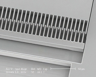
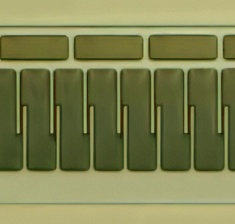
Release of comb drive structures
Stiction-free release of comb drives with 1 μm gap between adjacent comb fingers.
[source: idonus sàrl]
|
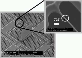
Structure thinning
Consecutive oxidation and HF VPE enables the fabrication of sub-micron diameter torsion beams.
[source: IMT, University of Neuchâtel]
|
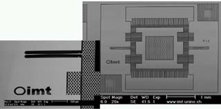
Dicing free Release of Optical MEMS
Intelligent double sided deep reactive ion etching enables dicing free release of chips on wafer level.
[source: IMT, University of Neuchâtel]
|
Isle structures
Timed etching allows the fabrication of isle structures (bright) that are only suspended by the remaining
SiO2. The darker structures are released.
[source: IMT, University of Neuchâtel]
|
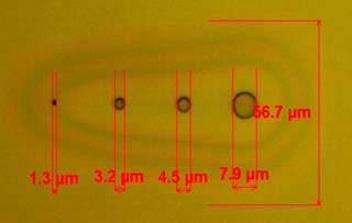
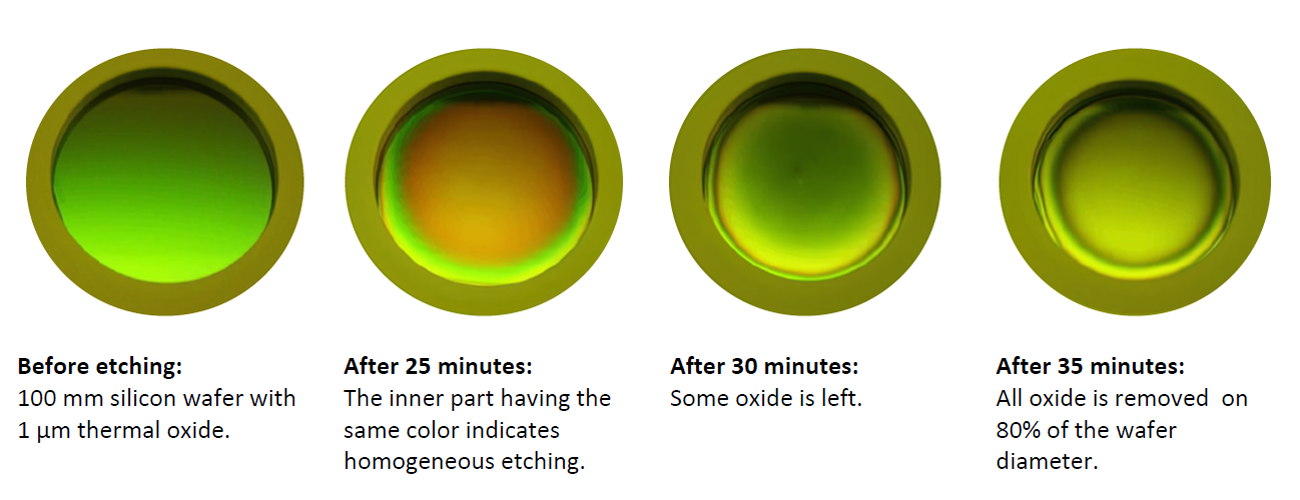
Etch rates of small openings
The holes were dry-etched into 0.5 μm of polysilicon deposited on 1 μm of thermal SiO2.
The etch rate of the sacrificial SiO2 depends on the diameter of the opening. Neither sticking nor "bad wetting"
(liquids that do not diffuse into small holes) of the small openings occurred.
[source: idonus sàrl]
|
Photonic bandgap
Nanometric membranes on thin sacrificial layers can easily be released
[source: IMT, University of Neuchâtel]
|
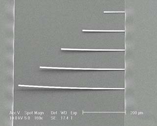
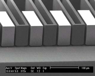
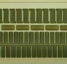
Thin film applications
0.5 μm thick polysilicon beams released on 1 μm thermal SiO2:
The width of the beams is 10 μm the length varies from 100 to 500 μm.
[source: idonus sàrl]
|
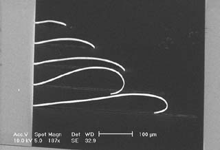
Aluminum structures
Aluminum structures on SiO2 can be released.
The high stress in the aluminum cantilevers causes a strong curling.
The 0.5 μm thick aluminum layer was deposited on 1 μm thermal SiO2.
[source: idonus sàrl]
|
|
.jpg)
Polymer-ceramic MEMS bimorph
The oxide hard mask covering the structures (paddle, thermal isolation linkages, and anchors)
is visible prior to HF etching and is yellow in color. Once etched away, it reveals the polysilicon beneath.
After completion of the etching of the sacrificial layer, the inner bimorph beams and the thermal isolation
regions are released and bend.
[source: C.G. Warren / UC Berkeley ]
Click on the illustration to watch a short animation of this HV vapor release.
|
.jpg)
Silicon nanowires
Ultra-high aspect ratio nanowires were obtained by HF vapor etching with the idonus VPE by researchers from the Paul Scherrer Institute (PSI).
DOI: 10.1039/C9NH00709A
[source: L. Romano / PSI, 2020]
See our dedicated newsletter (06/2020)
|

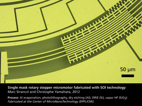
SOI micromotor
This 3-phase electrostatic rotary stepper micromotor was fabricated with SOI technology using a single mask. For this purpose, moving structures were
patterned with etch holes to ensure complete etching of the buried oxide layer (SiO2) by vapor HF (using the idonus VPE 100).
DOI: 10.1109/ JMEMS.2012.2189367
[source: M. Stanczl and C. Yamahata / EPFL, 2012]
Click on the illustration to watch a short animation of this MEMS device at work.
|

.gif)